
Tập tin:NE555 Bloc Diagram.svg

Tập tin gốc (tập tin SVG, 723×524 điểm ảnh trên danh nghĩa, kích thước: 32 kB)
Miêu tả
| Miêu tả |
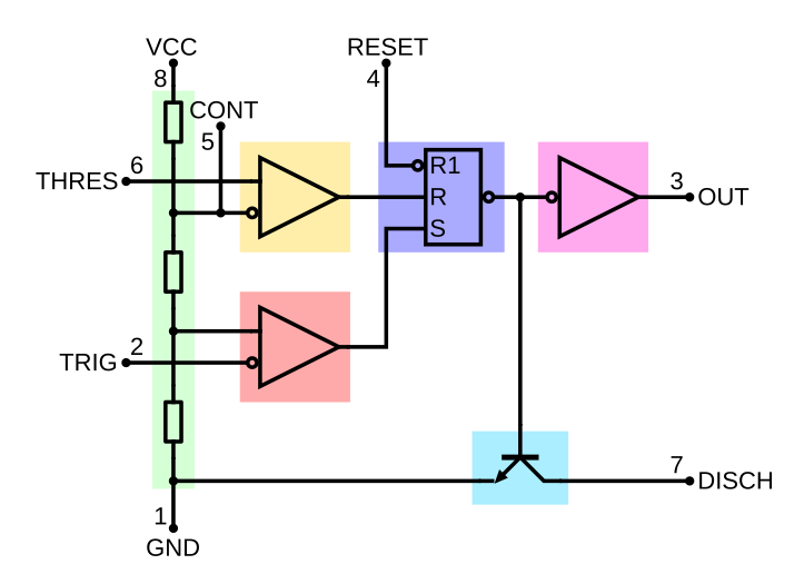
English: The NE555 contains 24 bipolar transistors, two diodes and 15 resistors that form six functional blocks:
Between the supply voltage VCC (+) and the ground GND (-) is a voltage divider consisting of three identical resistors which, when connected not from the outside, the two reference voltages ¹ / 3 VCC and ² / 3 VCC supplies. The latter is at the terminal pin Control Voltage available. The block diagram and schematic that area is highlighted in green. Two comparators are each connected to one of the reference voltages, while the other two inputs of which are fed directly to the terminals of trigger or threshold. The block diagram in yellow and orange. A flip-flop, deposited in the color purple, stores the state of the timer and is controlled by the two comparators. Via the reset terminal overrides the other two inputs, the flip-flop (and therefore the entire timer device) be reset at any time. At the output of flip-flop followed by an output stage with totem-pole output that can be loaded at the port output with up to 200 mA. Shown in the color pink. Parallel to the output stage of a transistor is connected, the collector is located on the discharge port. The transistor in the circuit diagram is a light blue background, always energized when the output is low level.Deutsch: Der NE555 enthält 24 Bipolartransistoren, zwei Dioden und 15 Widerstände, die zusammen sechs Funktionsblöcke bilden:
|
| Ngày | |
| Nguồn gốc | Tác phẩm được tạo bởi người tải lên |
| Tác giả | BlanchardJ |
| Phiên bản khác |
  |
Giấy phép
| Tôi, người giữ bản quyền của tác phẩm này, chuyển tác phẩm này vào phạm vi công cộng. Điều này có giá trị trên toàn thế giới. Tại một quốc gia mà luật pháp không cho phép điều này, thì: Tôi cho phép tất cả mọi người được quyền sử dụng tác phẩm này với bất cứ mục đích nào, không kèm theo bất kỳ điều kiện nào, trừ phi luật pháp yêu cầu những điều kiện đó. |
Lịch sử tập tin
Nhấn vào ngày/giờ để xem nội dung tập tin tại thời điểm đó.
| Ngày/Giờ | Hình xem trước | Kích cỡ | Thành viên | Miêu tả | |
|---|---|---|---|---|---|
| hiện tại | 19:54, ngày 16 tháng 1 năm 2012 | | 723×524 (32 kB) | Wdwd | Colored function blocks (for circiut diagram) correct transistor symbol (without a circle, because it's inside the chip) |
| 23:27, ngày 7 tháng 6 năm 2009 |  | 723×524 (40 kB) | Brighterorange | remove spurious red dot | |
| 20:22, ngày 23 tháng 9 năm 2007 |  | 723×524 (40 kB) | BlanchardJ | {{Information |Description=Bloc diagram of a 555 timer IC |Source=self-made |Date=September 23 2007 |Author=BlanchardJ |Permission= |other_versions= }} {{Created with Inkscape}} {{ElCompLib}} Category:555 timer IC |
Trang sử dụng tập tin
6 trang sau sử dụng tập tin này:
Sử dụng tập tin toàn cục
Những wiki sau đang sử dụng tập tin này:
- Trang sử dụng tại ar.wikipedia.org
- Trang sử dụng tại beta.wikiversity.org
- Trang sử dụng tại ca.wikipedia.org
- Trang sử dụng tại cs.wikipedia.org
- Trang sử dụng tại cs.wikibooks.org
- Trang sử dụng tại de.wikipedia.org
- Trang sử dụng tại en.wikipedia.org
- Trang sử dụng tại es.wikipedia.org
- Trang sử dụng tại et.wikipedia.org
- Trang sử dụng tại fa.wikipedia.org
- Trang sử dụng tại fi.wikipedia.org
- Trang sử dụng tại fr.wikipedia.org
- Trang sử dụng tại fr.wikiversity.org
- Trang sử dụng tại he.wikipedia.org
- Trang sử dụng tại hi.wikipedia.org
- Trang sử dụng tại hu.wikipedia.org
- Trang sử dụng tại id.wikipedia.org
- Trang sử dụng tại it.wikipedia.org
- Trang sử dụng tại ja.wikipedia.org
- Trang sử dụng tại lt.wikipedia.org
- Trang sử dụng tại no.wikipedia.org
- Trang sử dụng tại pl.wikipedia.org
- Trang sử dụng tại pt.wikipedia.org
- Trang sử dụng tại ru.wikipedia.org
- Trang sử dụng tại uk.wikipedia.org
- Trang sử dụng tại zh.wikipedia.org